New Chip-Scale Optical Platform Enables High-Quality Ultrawide Beam Steering
Integrating a light-routing chip, microscopic reflectors, and a metasurface enables high-quality two-dimensional
Press Release Disclaimer: This is a press release distributed through the XPR Media network. It has not been independently verified by our newsroom.
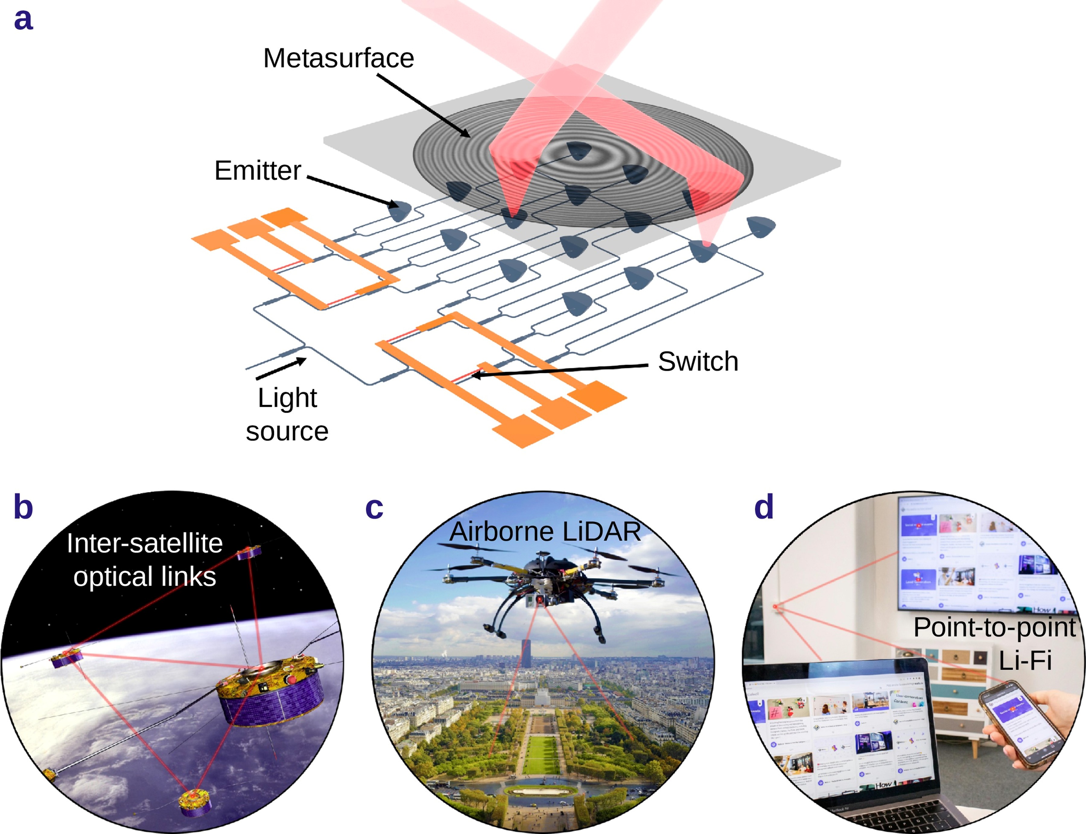

Integrating a light-routing chip, microscopic reflectors, and a metasurface enables high-quality two-dimensional optical beam steering across 161 degrees
CHENGDU, SICHUAN, CHINA, September 14, 2026 /EINPresswire.com/ — Researchers have developed a chip-scale platform for ultrawide-angle, two-dimensional optical beam steering. The system integrates a silicon photonic integrated circuit, freeform micro-optical reflectors, and a metasurface to transform guided light into high-quality free-space beams and direct them across a measured 161° field-of-view while maintaining nearly diffraction-limited beam quality. This compact, scalable architecture offers a pathway toward inter-satellite optical links, airborne LiDAR, point-to-point optical wireless communications, and other applications requiring agile, wide-angle beam control.
Directing an optical beam to a chosen location is central to many free-space systems. Satellites must acquire and track one another as their relative positions change, airborne LiDAR must scan broad landscapes, optical wireless links must reach receivers at different locations, and collaborative robots may need to sense or communicate across a scene.
These tasks require steering in both horizontal and vertical directions while keeping the beam narrow. Mechanical scanners can cover large angles, but they add size, weight, power consumption, and moving parts. Chip-based optical phased arrays reduce mechanical motion, yet most scan widely in only one direction. Extending them to true two-dimensional operation can require densely packed arrays and large numbers of individually controlled elements, greatly increasing electrical complexity and energy use.
Professor Juejun Hu’s research group at the Massachusetts Institute of Technology (MIT), USA, and the Singapore-MIT Alliance for Research and Technology (SMART), Singapore, together with collaborators, has developed and demonstrated a hybrid photonic platform that addresses a longstanding challenge in optical beam steering: achieving a wide two-dimensional field-of-view without sacrificing beam quality or requiring an impractically complex control system. Their work was made available online on August 23, 2026, in the Early View section of Opto-Electronic Advances journal.
The research team pursued a different approach inspired by optical projection. Instead of controlling a dense array of optical antennas, a silicon photonic integrated circuit routes light through a network of switches to a selected output waveguide, where a freeform micro-optical reflector turns the light upward into a clean free-space beam.
“The beam then passes through a metasurface patterned with nanoscale structures,” says Prof. Hu. “The position of the selected reflector determines the direction in which the metasurface sends the beam, so choosing a different optical path directly produces a different steering direction.”
The platform was developed by combining analytical optical design, numerical modeling, established semiconductor manufacturing, three-dimensional microprinting, and nanofabrication. The photonic integrated circuit was produced using a standard silicon photonics foundry process. The reflectors were designed to efficiently transform the guided optical mode into a Gaussian-like free-space beam and were printed directly on the chip.
The metasurface pattern was first established through an analytical design framework and then refined using optical simulations to reduce aberrations at large steering angles. After careful assembly and alignment, the system was tested at telecommunications wavelengths. It achieved two-dimensional steering over a measured 161° field-of-view while maintaining nearly diffraction-limited beam quality across a broad angular range.
The architecture offers several clear paths forward for further improvement. Compact piezoelectric translation could add fine or continuous steering between the discrete directions provided by the current reflector array, while lower-loss photonic foundry processes, improved alignment, and direction-specific metasurface optimization could enhance overall optical efficiency. Increasing the effective aperture or pairing the platform with beam-expanding optics could also narrow the output beam for long-distance operation.
“These advances will build on the demonstrated wide field-of-view and high beam quality,” notes Prof. Hu, “moving the technology toward scalable optical projectors for communications, sensing, and other applications requiring agile, wide-angle control of light.”
***
Reference
Title of original paper: Ultrawide-angle diffraction-limited 2D beam steering via hybrid integrated metasurface-photonic circuit
Journal: Opto-Electronic Advances
DOI: 10.29026/oea.2026.260099
About Opto-Electronic Advances
Launched in March 2018, Opto-Electronic Advances (OEA) is an open-access, peer-reviewed SCI journal. Indexed in major databases including SCI, EI, and Scopus, it is guided by an international editorial board spanning 17 countries. OEA provides a fast-track platform for high-impact empirical and theoretical research across optics, photonics, and optoelectronics. Key focus areas include light sources, sensors, nanophotonics, plasmonics, biophotonics, optical imaging, intelligent optics, and optical communications, catering to researchers, academicians, and industry professionals seeking cutting-edge developments in light-driven technologies.
Website: https://www.oejournal.org/oea/en/
About Professor Juejun Hu’s research group at the Massachusetts Institute of Technology (MIT), USA
Professor Juejun Hu’s research group at MIT focuses on two main areas: integrated photonics and metasurface optics. In integrated photonics, the group develops novel photonic packaging technologies and on-chip spectroscopic sensing methods, while exploring heterogeneous integration approaches for seamlessly incorporating new materials—including nonvolatile phase-change materials, magneto-optical and electro-optic crystals, and nontraditional polymer and semiconductor materials—into standard foundry fabrication processes. In metasurface optics, the group’s research spans design theory and algorithms, nanofabrication, and the integration and packaging of metasurfaces with other optoelectronic components to support applications in imaging, sensing, displays, optical communications, and LiDAR. Across both areas, the group combines optical design, materials, fabrication, and integration to translate scientific advances into compact, scalable, and practical photonic systems.
Funding information
The authors are grateful for financial support from Singapore MIT Alliance for Research and Technology centre under the Wafer-scale Integrated Sensing Devices based on Optoelectronic Metasurfaces (WISDOM) Program, NASA STTR Phase I Contract 80NSSC23PB289, and Air Force Office of Scientific Research under award number FA23862614003.
Siyi Ma
Institute of Optics and Electronics, CAS
+86 191 3618 6296
oej_publishing@ioe.ac.cn
Legal Disclaimer:
EIN Presswire provides this news content “as is” without warranty of any kind. We do not accept any responsibility or liability
for the accuracy, content, images, videos, licenses, completeness, legality, or reliability of the information contained in this
article. If you have any complaints or copyright issues related to this article, kindly contact the author above.

Media gallery